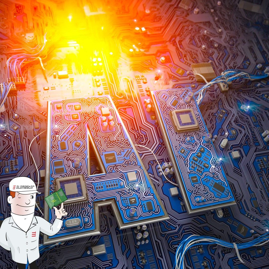
Every prompt sent to a chatbot reaches something physical: a server rack inside a data centre. Within that rack, the processors that make artificial intelligence work are mounted on printed circuit boards that may look, at first sight, like the green boards used in any electronic product.
In reality, they are very different. AI server boards are among the most complex products the electronics industry has ever had to manufacture, and the race to build them is changing the PCB sector. This is one of the topics at the centre of the discussions among the professionals gathering at PCB West in California, where the Elemaster Group will be represented by Eleprint, the group company specialising in PCB manufacturing.
From twenty layers to forty, and beyond
A conventional multilayer PCB is built as a sandwich of copper, resin and woven glass fibre, laminated into a rigid board that usually measures between 1.6 and around 3.5 mm in thickness. With up to 20-22 layers, this structure has supported around 99% of electronic applications so far, from defence and aerospace to medical devices and telecommunications.
AI server boards change this scale. Current designs already range from 20 to 40 layers, while the most advanced solutions go far beyond that. In 2025, Japan’s OKI Circuit Technology announced a 124-layer, 7.6 mm board designed for testing the high-bandwidth memory used in AI chips.
Because nothing inside the stack can be compressed, every additional layer increases thickness. Once boards move beyond 40 layers, they exceed 4-5 mm, while the most complex designs can reach 7-8 mm.
Millions of connections on one board
Layer count is only part of the challenge. The GPUs and AI accelerators mounted on these boards, each with thousands of pins, need to exchange data with each other and with the rest of the system at speeds of up to 28 gigabits per second on a single trace.
To make this possible, two advanced techniques need to work together. Sequential build-up grows the board step by step, laminating new layers around an inner core instead of pressing the entire stack at once. High-density interconnection, known as HDI, connects those layers through through-holes, blind vias that link only adjacent layers and buried vias hidden inside the stack.
Together, these processes make it possible to create millions of interconnections on a single, highly miniaturised board.
Why one board in three is scrapped
The technology is still far from mature. For more than thirty years, hardware has struggled to keep pace with software, and AI has widened that gap even further.
A single AI board can include 25,000 through-holes and 45,000 blind or buried vias. If just one hole out of 70,000 is plated incorrectly, the entire board becomes unusable. For this reason, industrial yields of 60-70% are common, meaning that roughly one board in three is discarded. In standard production, by comparison, scrap rates are usually between 1% and 3%.
This gap is one of the reasons these boards cost far more than conventional ones.
Thickness creates another obstacle. More than 90% of PCB manufacturers worldwide are currently unable to process boards thicker than 6-7 mm. Moving beyond that threshold requires custom machinery and significant investment.
Heat and signal integrity
Heat is another major issue. Next-generation AI processors, operating with data rates of 1.6 terabits per second, can exceed 120-130 °C, creating risks for the chip itself and for the components around it.
A multilayer board is made from different materials, and this means it does not conduct heat efficiently. To manage this, designers increasingly use metal coins, solid inserts as thick as the board itself, to move heat away. They may also add thermal vias, whose only role is to spread heat towards the bottom of the board and prevent hot spots.
These decisions are often developed through co-engineering between the customer and the PCB manufacturer.
“One of our most recent investments was precisely in lamination systems able to handle exotic materials: with the traditional presses we had until a few years ago, we simply could not process them. The challenges of AI applications are global, and they mostly involve enormous groups. For us it is David against Goliath, but it is a challenge we accept willingly” says Paolo Potenza, COO & CTO at Eleprint.
An Italian player among giants
This field is dominated either by very large groups or by highly specialised niche companies. Eleprint, the PCB manufacturing company of the Elemaster Group, based in Montevecchia, Lombardy, has chosen to take on the challenge.
The company has invested in new lamination systems capable of processing exotic materials, in sequential build-up with up to five consecutive pressing cycles, including blind, buried and blind-buried vias, and in controlled-depth drilling along the Z axis.
The next frontier the group is looking at is moving beyond 40 layers, towards boards between 6.5 and 7.3 mm thick. On the assembly side, Elemaster is already equipped to mount GPUs with thousands of pins, a process that requires five to seven stages, compared with the 120-130 process steps needed to manufacture the board itself.
See it at PCB West 2026
These are the themes Eleprint will bring to PCB West 2026, at the Santa Clara Convention Center in California. The conference runs from 29 September to 2 October, while the exhibition opens on 30 September.
For Eleprint, representing the Elemaster Group in Silicon Valley, the event is an opportunity to show that a Lombard manufacturer can compete in one of the most demanding areas of electronics.