
What is PCB? What does PCB mean? PCB, acronym of Printed Circuit Board, electrically connects and mechanically supports electrical and/or electronic components. The name explains himself; copper tracks (the Circuit) gets printed on a Board using a set of mechanicals, chemicals and physicals processes.
PCB are at the base of almost all of electronic products .
Components are generally soldered onto the PCB to both electrically connect and mechanically fasten them to it to produce a PCBA [Printed Circuit Board Assembly]
In standard PCB the mechanical support is provided by electrically insulating materials, the electrical connection between components by copper tracks.
A PCB is basically one or more sheet layers of copper [typically between 9 and 210 micrometers] sandwiching sheet layers of a non-conductive substrate [typically between 0,8 and 3,6 millimeters].
Characteristics of PCB
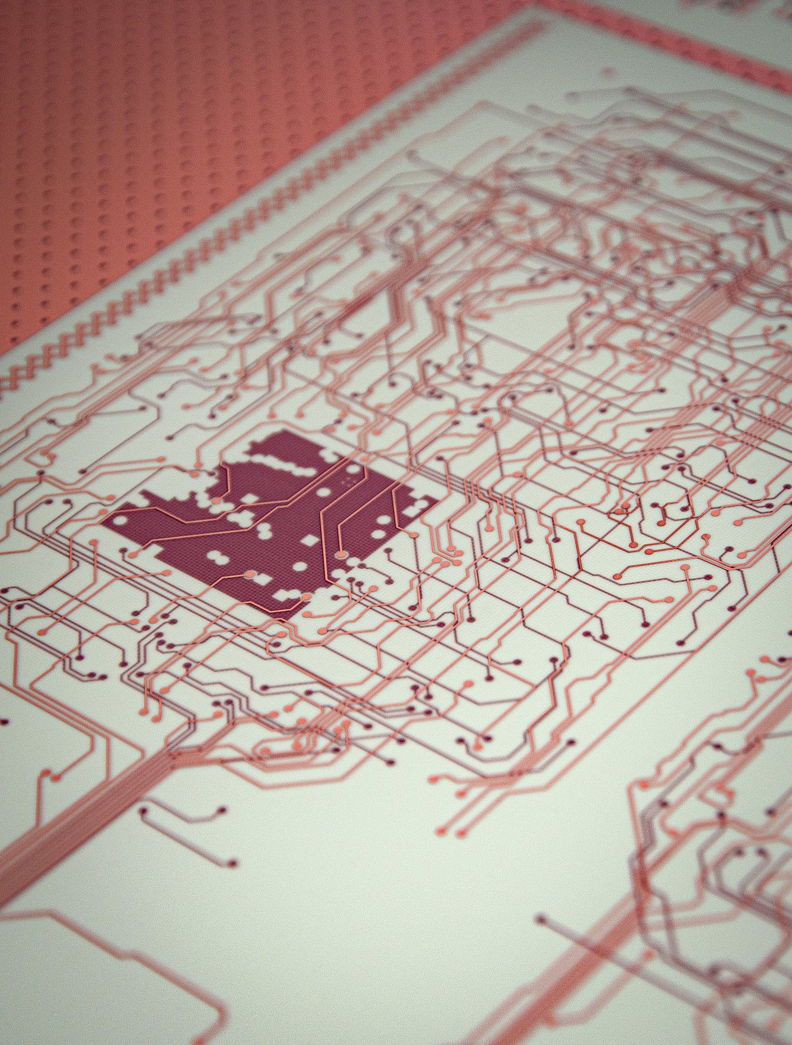
The simplest PCB are single sided. Copper tracks take just one side of the board [One Layer].
Two sides PCB [Two Layers] have copper tracks on both the sides of a board. To electrically connect different layers. Holes with metallized walls are drilled throughout the board to electrically connect the layers.
When a PCB has more than two layers, is called a multilayer PCB. It hosts copper tracks not only on the board external sides but inside the board too.
To protect the tracks from mechanical, chemical damage or undesired electrical contact, a coating protects the PCB surface. For its function in helping to prevent solder shorts, the coating is called “solder resist” or “solder mask”.
The mask covers all copper traces but the “pads”, little island of copper, site where components will be soldered over.
To help the soldering of components on PCB’s pads, a thin metal layer is deposited on pads.

Different types of PCB
Different technologies of PCB are offered on the market. Those PCBs differ for number of layers, thickness, size,
base material [the insulating material the board is made of]:
- glass epoxy;
- cotton paper;
- ceramic;
- polyamide based materials
- Polytetrafluoroethylene (PTFE);
finishing [the metallic layer that coats pads helping to solder components]:
- Tin and Lead alloy;
- Tin and Silver alloy;
- Chemical deposited silver
- Chemical deposited tin
- Chemical deposited gold over a layer of electrodeposited Nichel;
A main subdivision of PCB could be:
- Rigid PCBs
- Flex PCBs
- Rigid-Flex PCBs
Where Rigid PCBs are made of “hard” base materials, Flex PCBs are PCB that have a base material made out of e.g. polyamide and can be folded, Rigid-Flex are PCBs with made of base materials with rigid and flexible parts.
The most recent class of PCBs are HDI [High Density Interconnect] PCB. HDI PCB could contain blind and/or buried vias and often contain holes of 150 microns or fewer in diameter, have a higher circuitry density than standard PCBs.

How to make PCB
PCBs industrial manufacturing.
The PCB production involves mechanical, chemical and physical processes.
Production steps of a double layer FR4 PCB could be resumed as:
A laminate, two copper foil sandwiching a slab of glass-epoxy is drilled;
Holes are cleaned from drilling residues;
A photo sensible film is laid over the PCB;
Tracks and pads shape is imaged on the photo sensible film;
The photo sensible film is “developed”, light exposed parts are worn off by chemicals;
A galvanic process adds copper over exposed parts and over holes walls;
Tin is electrochemically added to protect the exposed copper;
The remaining film is worn off by chemicals, this exposes the previously protected copper;
The now exposed copper is worn of by chemicals, letting only the tin protected copper on both sides of the board;
The tin too is worn off by chemicals;
The board gets covered by solder mask coating;
The solder mask shape is imaged on the board;
The solder mask is “developed”, light non-exposed parts are worn off by chemicals;
Metal finishing is added “bathing” the board in a chemical solution.
Routing gives the board its final physical shape;
The board is ready for testing, packing and shipping.
What is the use of PCB – Commercial uses of PCBs
Here are the main commercial uses of PCBs: these are classic and traditional uses. There are also many other uses and applications of PCBs.
- Transformers and capacitors;
- Electrical equipment, including voltage regulators, switches, reclosers, bushings and electromagnets;
- Oil used in engines and hydraulic systems;
- Old electrical devices or appliances containing PCB capacitors;
Why are PCB green
The green color of the PCBs is determined by the solder mask: the latter protects the copper circuits printed respectively on the glass fiber core, in order to avoid short circuits, soldering errors, and other problems. It is therefore the color of the solder mask that gives the board its classic appearance.
How is PCB designed
How does the PCB design process happen? PCB design begins with converting a schematic diagram into a physical circuit board layout. At the end of this operation, we proceed with a test concerning your problem-solving skills: in this regard, we proceed by placing the components in an extremely limited space.
H3 Which software is best for PCB design
Today there are a good deal of software software for the design of printed circuits on the market: free or paid software are available that operate from the prototyping phase to the industrialization of the product. Which software to choose among the many available on the market, able to meet your specific needs? Here is a short list of the main software available on the market:
- Protel (Altium designer)
- Orcad
- Pads (Power PCB)
- Eagle
- Kicad
- Allegro
- Fritzing
- EasyEda