How PCB manufacturing, assembly and industrialisation expertise contribute to smaller, lighter and more reliable electronic systems
Advanced electronics is evolving towards increasingly demanding architectures. IoT devices, AI-enabled systems, high-frequency circuits, aerospace platforms and next-generation healthcare technologies require printed circuit boards that are more compact, lighter, more reliable and capable of managing complex signals with stable performance.
Today, many PCBs operate at frequencies above the GHz range. At the same time, electronic systems are expected to occupy less space, reduce weight, improve energy efficiency and perform consistently in challenging operating environments.
This evolution is changing the role of the printed circuit board. In high-performance applications, the PCB is no longer simply the physical support on which electronic components are assembled. Its materials, internal architecture and production process have a direct influence on signal integrity, thermal behaviour, reliability and the overall performance of the final device.
This is particularly important in fields such as biomedical electronics and aerospace. In medical devices, miniaturisation can support better ergonomics, greater portability and, in some cases, the development of wearable or implantable systems. In satellites, spacecraft and advanced aerospace platforms, reducing weight and optimising internal space can directly affect system efficiency and mission performance.
What changes with embedded PCB technology
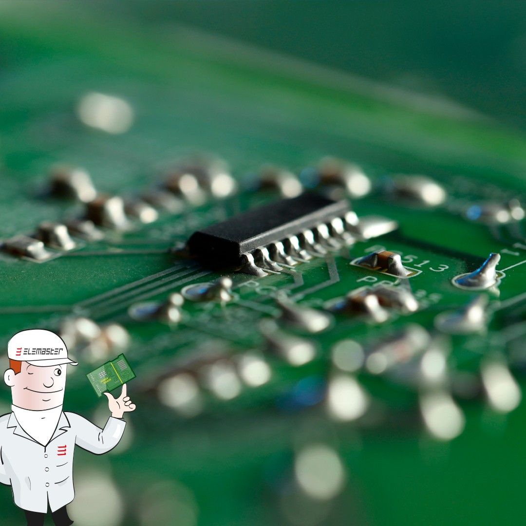
In a conventional PCB assembly flow, components are mounted on the surface of the board after the circuit has been produced. These components may be passive, such as resistors, capacitors and inductors, or active, such as chips and microchips, which process information and control the functions of the electronic system.
Embedded PCB technology changes this structure by integrating part of the componentry inside the multilayer architecture of the printed circuit board. Rather than placing all elements on the surface, selected components are incorporated within the PCB itself and covered by resin as part of the board structure.
The first application area concerns passive components. By integrating resistors, capacitors and other passive elements inside the PCB, the number of surface-mounted parts can be reduced and the board layout can be optimised. Depending on the application requirements, this approach can reduce the PCB surface area by up to 30% and decrease board weight by approximately 20-30%.
These reductions are especially significant in sectors where every millimetre and every gram can make a difference. In aerospace applications, lighter electronic assemblies can help reduce the total weight of a satellite, capsule or onboard system. In biomedical electronics, a more compact board can support devices that are easier to handle, integrate or miniaturise.
Embedded architectures also improve the electrical behaviour of the circuit. By shortening connection paths, they reduce parasitic effects and parasitic capacitance, limiting losses and improving signal integrity. This aspect becomes crucial in high-frequency applications, where the physical distance between components can influence signal quality and stability.
Thermal management is another important benefit. As frequency and power density increase, electrical losses generate heat that must be properly controlled inside the device. Embedded components, together with design solutions such as through holes, copper filling, metal cores or copper cores, can contribute to more effective heat management and help keep the circuit within the required operating conditions.
Reliability can also benefit from this approach. Reducing the number of surface-mounted components and soldering points means reducing some of the potential failure points within the assembly. Solder joints can be affected by corrosion, mechanical stress and long-term degradation. Integrating selected components inside the PCB can therefore contribute to a more robust architecture.
Why process control is essential in advanced PCB innovation
Embedding components into a printed circuit board is a complex process. It requires dedicated materials, controlled multilayer manufacturing and a clear understanding of how the board will behave during production, assembly and operation.
Passive embedded components, for example, require specific materials that make it possible to create resistors or capacitors within the circuit. The PCB manufacturer must be able to source these materials, process them correctly and control their performance throughout the full manufacturing cycle.
Layer alignment is one of the most sensitive aspects. In a multilayer PCB, each layer must be positioned with very high precision to ensure reliable interconnections and consistent electrical behaviour. The more complex the circuit, the more important it becomes to control material selection, lamination, drilling, registration, finishing and testing.
This level of complexity makes design review a key phase. The customer defines the functional requirements of the device, but these requirements must then be translated into an architecture that is both manufacturable and reliable. This demands continuous interaction between the customer, the design team, the PCB manufacturer and the assembly partner.
In this process, the PCB manufacturer becomes a technical partner. Its role is not limited to production. It also includes feasibility assessment, risk identification, design optimisation and support in reducing the cost and complexity of the final device before the product reaches the later stages of development.
Elemaster’s integrated approach to technical complexity
The development of embedded PCB technology shows clearly why advanced electronics increasingly depends on the integration of different areas of expertise. Materials knowledge, PCB manufacturing, design review, prototyping, assembly and industrialisation all influence the performance and reliability of the final product.
As Paolo Potenza, CTO of Eleprint, explains: “The market is moving towards electronic systems that work at higher frequencies, occupy less space and must remain reliable in increasingly demanding applications. Embedded technology responds to these needs, but it also requires a very close connection between PCB manufacturing know-how, material expertise, assembly capabilities and design review. This is where the structure of Elemaster Group becomes a competitive advantage: Eleprint brings advanced PCB expertise, while the Group adds the assembly and industrialisation competences needed to turn complex technologies into reliable products.”
Within the Group, Eleprint has developed solid know-how in advanced PCB manufacturing, complex multilayer structures and the integration of passive embedded components. This competence is particularly valuable in applications where miniaturisation, signal integrity and process reliability are critical.
At the same time, embedded technology is evolving towards more advanced architectures, including the integration of active components such as chips and microchips inside the PCB. This development requires an even stronger connection between PCB production and electronic assembly. Elemaster’s experience in assembly and industrialisation becomes a key resource for studying, developing and managing this next phase.
Eletech also contributes to this integrated model through design review, prototyping and feasibility analysis. Its role is to connect customer requirements with production constraints, helping optimise the product before it moves into full-scale manufacturing.
For customers, this means working with an industrial partner able to support the development path from the earliest design stages through to manufacturing and assembly. In technologies such as embedded PCB, this integration helps reduce risk, accelerate development and improve the manufacturability of advanced electronic systems.
Application focus: planar transformers for advanced medical devices
A concrete example of advanced PCB know-how applied to a real device comes from Eleprint’s activity in printed circuit boards for medical electronics.
Eleprint produces PCBs for different types of electromedical equipment, including systems for preventive eye diagnostics, dialysis treatment, cardiovascular applications and preventive blood diagnostics. In these fields, compactness, reliability and performance are essential for the final application.
One significant case concerns a section of a planar electronic transformer used in medical equipment. The circuit has an out-of-standard thickness of 6.5 mm and is produced as a 22-layer structure, with 6 active layers. This architecture was selected to achieve maximum planarity in the finished circuit.
The final transformer is obtained by assembling two circuits with ferrite plates, making it possible to achieve the required electrical coupling and operating voltage. The miniaturised PCB can be installed in restricted spaces, contributing to the handling and performance of the medical device.
This application is closely linked to the same technical drivers behind embedded PCB technology. It demonstrates how advanced multilayer design, miniaturisation and process control can enable more compact and higher-performing electronics. It also highlights the importance of managing complex PCB architectures, including blind mechanical vias and high interconnection density, with demanding aspect ratios.
For medical electronics, this capability directly affects product development. A smaller and more reliable PCB can support devices that are more compact, easier to use and better suited to advanced diagnostic or therapeutic applications.
Embedded PCB within a broader innovation strategy
Embedded PCB technology is one of the most relevant directions in advanced electronics. It is developing alongside other innovation paths, including new semi-additive processes, ultra-fine tracks, thinner circuits, flex and rigid-flex architectures.
Companies working in high-performance electronics need to evaluate these technologies according to concrete product requirements. The key is understanding which innovation can improve a specific device, how it can be industrialised and how it can be integrated into a reliable manufacturing process.
Elemaster Group’s expertise in embedded PCB technology reflects this approach. It shows how specialised know-how, cross-functional collaboration and industrial execution can make advanced technologies usable in real applications.
This is what makes the integrated model competitive. PCB manufacturing, design support, assembly and industrialisation are connected competences that shape the final product. For customers developing complex electronic systems, this connection can make the difference between a promising technology and a market-ready solution.