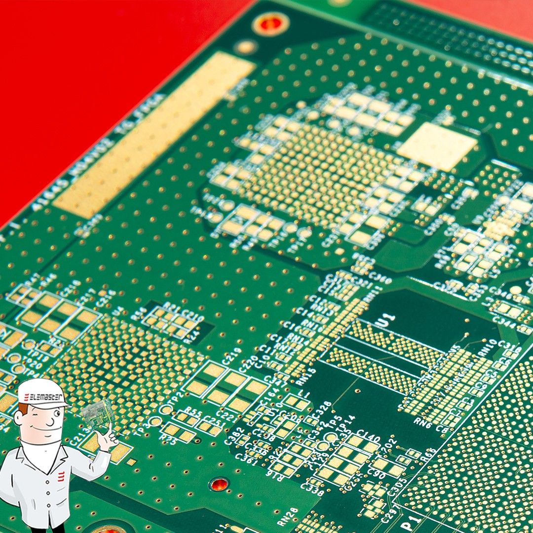
In the world of advanced electronics, the manufacturing of Printed Circuit Boards (PCBs) is a complex, multi-stage process that transforms an abstract design into a functional, reliable, and certified product. While a PCB may appear as a simple green laminate dotted with copper lines and components, its creation involves a sophisticated chain of operations that combine engineering expertise, industrial technologies, and rigorous quality controls.
This article explores the main stages of PCB manufacturing, highlighting how each step contributes to ensuring the high levels of performance and reliability required by modern industries.
From Concept to Design
The process begins with the design phase, where engineers translate the customer’s requirements into a functional electronic layout. This stage involves advanced CAD tools capable of defining the geometry of the conductive tracks, the positioning of the components, and the configuration of the layers.
During this phase, particular attention is paid to:
- Signal integrity, ensuring that high-frequency signals are not distorted.
- Thermal management, preventing overheating in power-dense areas.
- Design for Manufacturability (DfM) and Design for Testability (DfT), which simplify the subsequent production and validation stages.
The design stage is therefore crucial in aligning innovation with industrial feasibility, ensuring that the PCB can be manufactured efficiently and reliably.
Material selection and preparation
Once the design is validated, the focus shifts to the selection of materials. Depending on the sector of application, PCBs may require different substrates and laminates:
- FR4 fibreglass for standard boards.
- Aluminium-based substrates for applications with high thermal loads.
- Rogers laminates for high-frequency and RF applications.
The chosen materials are then cut and prepared to form the base of the board. This choice has a direct impact on performance, durability, and compliance with sector-specific standards.
PCB fabrication: from imaging to etching
At this stage, the design is physically transferred onto the board through a photolithographic process. A photosensitive film is applied to the copper surface, which is then exposed to UV light using the design mask. The exposed areas remain protected while the unexposed copper is chemically etched away, leaving behind the conductive tracks.
In multilayer PCBs, this process is repeated for each layer, which are then laminated together under heat and pressure to create a compact, reliable structure.
Key challenges in this stage include:
- Maintaining dimensional precision of tracks and vias.
- Avoiding defects such as short circuits or open circuits.
- Guaranteeing uniformity across multiple layers.
Drilling and plating
Once the layers are formed, the next critical operation is drilling. Tiny holes, often less than 0.2 mm in diameter, are drilled to create connections (vias) between layers. These vias are then metallised through electrolytic plating, which coats the interior walls with copper to ensure electrical conductivity.
This stage is particularly important in High-Density Interconnect (HDI) PCBs, where the miniaturisation of vias is essential to achieve compact and high-performance designs.
Solder mask and surface finishes
To protect the copper traces from oxidation and accidental short circuits, a solder mask is applied. This green (or sometimes blue, red, or black) coating also helps guide the soldering process by exposing only the pads where components will be mounted.
The exposed pads are then treated with surface finishes to improve solderability and reliability over time. Common finishes include:
- HASL (Hot Air Solder Levelling), cost-effective and widely used.
- ENIG (Electroless Nickel Immersion Gold), ensuring excellent planarity and durability.
- OSP (Organic Solderability Preservative), eco-friendly and reliable for specific applications.
Assembly: SMD and THT technologies
With the board fabricated, the next step is the assembly of electronic components. This can involve:
- Surface-Mount Device (SMD) technology, where components are soldered directly onto pads.
- Through-Hole Technology (THT), where component leads are inserted into drilled holes and soldered.
Automated pick-and-place machines ensure precision and speed in SMD assembly, while wave soldering or selective soldering systems manage THT processes. Often, both techniques are combined to accommodate complex designs.
Testing and quality control
No PCB is complete without rigorous testing and validation. This stage ensures that every board meets the required electrical, mechanical, and thermal specifications.
The main methods include:
- In-Circuit Testing (ICT), verifying component placement and electrical connections.
- Functional Testing, simulating real operating conditions.
- X-ray inspection, essential for detecting hidden soldering defects, particularly in BGAs.
- Burn-in tests, stressing the PCB under extreme conditions to verify long-term reliability.
For mission-critical sectors such as medical, railway, and aerospace, these tests are not optional but a fundamental requirement for certification and compliance.
Eleprint: the PCB excellence of the Group
Within the Elemaster ecosystem, Eleprint plays a central role in the production of high-precision PCBs. Specialised in rigid, flexible, rigid-flex, and multilayer solutions, Eleprint combines cutting-edge technology with industrial reliability. Its expertise ensures that every PCB complies with customer-specific requirements and international certifications, making it a strategic hub for the Group’s advanced electronic manufacturing capabilities.
Sustainability and lifecycle management
Modern PCB manufacturing also integrates sustainability principles. This includes the use of eco-friendly materials, the reduction of waste in chemical processes, and the optimisation of energy consumption across production lines.
Equally important is lifecycle management, which ensures continuity of supply, obsolescence management, and long-term support for products that may remain in operation for decades, such as in railway or aerospace sectors.
PCBs as enablers of industrial excellence
The PCB manufacturing process is a journey that begins with a design concept and culminates in a fully functional, reliable, and certified electronic product. Each stage, from imaging to assembly and testing, plays a decisive role in shaping the final outcome.
As industries continue to demand greater miniaturisation, higher performance, and uncompromising reliability, the importance of advanced PCB manufacturing will only grow.
Companies that can integrate design, production, testing, and lifecycle management within a unified industrial ecosystem are best positioned to deliver innovative solutions that stand the test of time.